General Description
This user guide contains information for the RTQ2806A DC-DC converter. Also included are the performance specifications, the schematic, and the list of materials for the RTQ2806A.
Performance Specification Summary
A summary of the RTQ2806A Evaluation Board performance specification is provided in Table 1. The ambient temperature is 25°C.
Table 1. RTQ2806A Evaluation Board Performance Specification Summary
|
Specification
|
Test Conditions
|
Min
|
Typ
|
Max
|
Unit
|
|
Input Voltage Range
|
|
3.5
|
12
|
17
|
V
|
|
Output Current
|
|
0
|
--
|
6
|
A
|
|
Default Output Voltage
|
|
--
|
1.8
|
--
|
V
|
|
Operation Frequency
|
|
--
|
1100
|
--
|
kHz
|
|
Output Ripple Voltage
|
IOUT = 6A
|
--
|
10
|
--
|
mVp-p
|
|
Line Regulation
|
IOUT = 3A, VIN = 3.5V to 17V
|
--
|
±0.5
|
--
|
%
|
|
Load Regulation
|
VIN = 12V, IOUT = 0.001A to 6A
|
--
|
±0.5
|
--
|
%
|
|
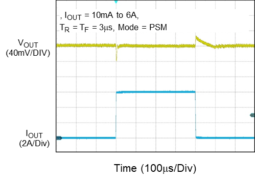
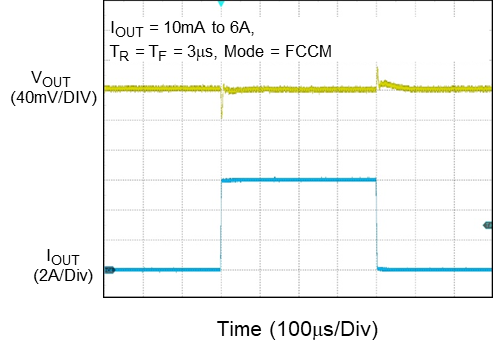
Load Transient Response
|
IOUT = 10mA to 6A
|
--
|
±5
|
--
|
%
|
|
Maximum Efficiency
|
VIN = 12V, VOUT = 1.8V, IOUT = 6A
|
--
|
89.6
|
--
|
%
|
Power-up Procedure
Suggestion Required Equipments
- RTQ2806A Evaluation Board
- DC power supply capable of at least 17V and 7A
- Electronic load capable of 6A
- Function Generator
- Oscilloscope
Quick Start Procedures
The Evaluation Board is fully assembled and tested. Follow the steps below to verify board operation. Do not turn on supplies until all connections are made. When measuring the output voltage ripple, care must be taken to avoid a long ground lead on the oscilloscope probe. Measure the output voltage ripple by touching the probe tip and ground ring directly across the last output capacitor.
Proper measurement equipment setup and follow the procedure below.
1) With power off, connect the input power supply to the VIN and GND pins.
2) With power off, connect the electronic load between the VOUT and nearest GND pins.
3) Turn on the power supply at the input. Make sure that the input voltage does not exceeds 17V on the Evaluation Board.
4) Check for the proper output voltage using a voltmeter.
5) Once the proper output voltage is established, adjust the load within the operating ranges and observe the output voltage regulation, ripple voltage, efficiency, and other performance.
Detailed Description of Hardware
Headers Description and Placement
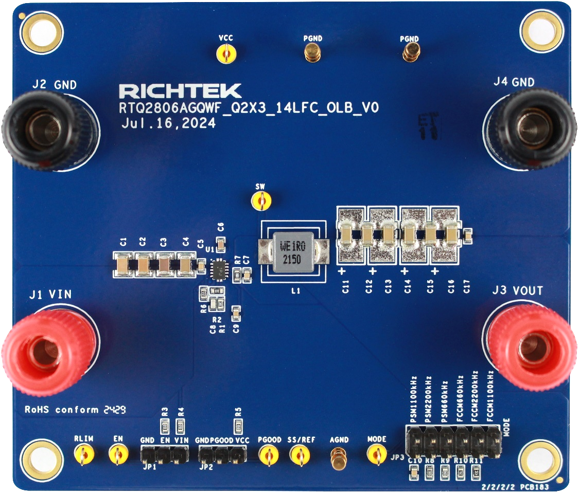
Carefully inspect all the components used in the EVB according to the following Bill of Materials table, and then make sure all the components are undamaged and correctly installed. If there is any missing or damaged component, which may occur during transportation, please contact our distributors or e-mail us at evb_service@richtek.com.
Test Points
The EVB is provided with the test points and pin names listed in the table below.
|
Test Point/
Pin Name
|
Function
|
|
J1
|
VIN input voltage connector
|
|
J2
|
PGND connection for input
|
|
J3
|
VOUT output voltage connector
|
|
J4
|
PGND connection for output
|
|
JP1
|
Connects EN to VIN to enable the device.
|
|
JP2
|
Connects PGOOD to VCC through a 100kΩ.
|
|
JP3
|
Mode selection
|
|
EN
|
EN test point
|
|
SS/REF
|
Can be used to monitor the reference voltage.
|
|
VCC
|
VCC test point
|
|
PGOOD
|
PGOOD output test point
|
|
MODE
|
Mode selection test point
|
|
RLIM
|
Can be used to monitor the voltage level of the valley current limit.
|
|
SW
|
Switch node test point
|
Bill of Materials
|
VIN = 12V, VOUT = 1.8V, IOUT = 6A, fSW = 1100kHz
|
|
Reference
|
Count
|
Part Number
|
Value
|
Description
|
Package
|
Manufacturer
|
|
U1
|
1
|
RTQ2806AGQWF
|
--
|
Step-Down Converter
|
WQFN-14TL 2x3 (FC)
|
RICHTEK
|
|
L1
|
1
|
74437346010
|
1µH
|
Inductor, Isat = 29A, 10mΩ
|
--
|
Wurth Elektronik
|
|
C1, C2
|
2
|
GRM31CR71E106KA12L
|
10µF
|
Capacitor, Ceramic, 25V, X7R
|
1206
|
MURATA
|
|
C3, C4
|
2
|
GRM31CR71H475KA12L
|
4.7µF
|
Capacitor, Ceramic, 50V, X7R
|
1206
|
MURATA
|
|
C5, C7, C10, C17
|
2
|
C1608X7R1H104KT000N
|
0.1µF
|
Capacitor, Ceramic, 50V, X7R
|
0603
|
TDK
|
|
C6
|
1
|
GRM188R61E475KE11D
|
4.7µF
|
Capacitor, Ceramic, 25V, X5R
|
0603
|
MURATA
|
|
C8
|
1
|
0603N331J500CT
|
330pF
|
Capacitor, Ceramic, 50V, NPO
|
0603
|
WALSIN
|
|
C9
|
1
|
GRM188R71H223KA01D
|
22nF
|
Capacitor, Ceramic, 50V, X7R
|
0603
|
MURATA
|
|
C11, C12,
C13, C14,
C15, C16
|
6
|
GRM31CR60J476ME19L
|
47µF
|
Capacitor, Ceramic, 6.3V, X5R
|
1206
|
MURATA
|
|
R1
|
1
|
WR06X2002FTL
|
20k
|
Resistor, Chip, 1/10W, 1%
|
0603
|
WALSIN
|
|
R2
|
1
|
WR06X1002FTL
|
10k
|
Resistor, Chip, 1/10W, 1%
|
0603
|
WALSIN
|
|
R3, R4, R5
|
3
|
WR06X1003FTL
|
100k
|
Resistor, Chip, 1/10W, 1%
|
0603
|
WALSIN
|
|
R6
|
1
|
RC0603FR-075K1L
|
5.1k
|
Resistor, Chip, 1/10W, 1%
|
0603
|
YAGEO
|
|
R7
|
1
|
WR06X000 PTL
|
0
|
Resistor, Chip, 1/10W, 1%
|
0603
|
WALSIN
|
|
R8
|
1
|
WR06X2433FTL
|
243k
|
Resistor, Chip, 1/10W, 1%
|
0603
|
WALSIN
|
|
R9
|
1
|
RTT031213FTP
|
121k
|
Resistor, Chip, 1/10W, 1%
|
0603
|
RALEC
|
|
R10
|
1
|
CR0603F60K4P05Z
|
60.4k
|
Resistor, Chip, 1/10W, 1%
|
0603
|
EVER OHMS
|
|
R11
|
1
|
RTT033012FTP
|
30.1k
|
Resistor, Chip, 1/10W, 1%
|
0603
|
RALEC
|
Typical Applications
EVB Schematic Diagram
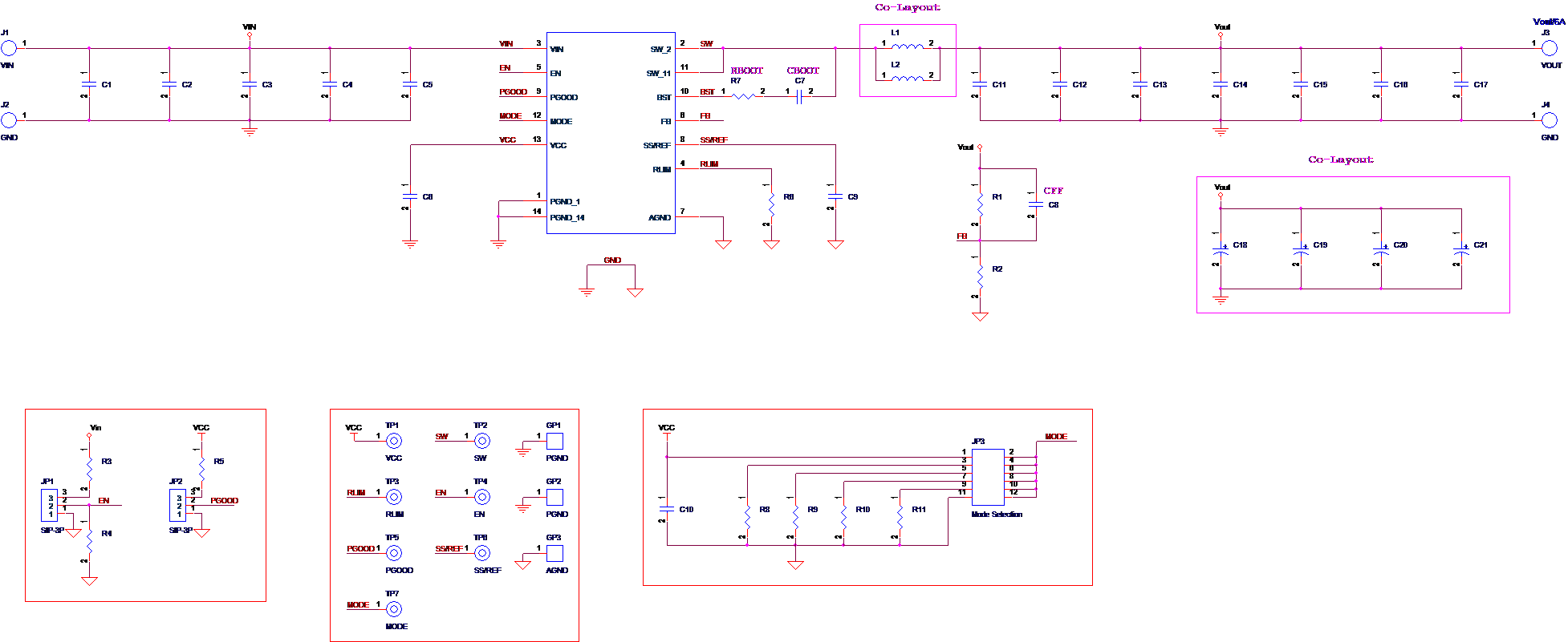
1. The capacitance values of the input and output capacitors will influence the input and output voltage ripple.
2. MLCC capacitors have degrading capacitance at DC bias voltage, and especially smaller size MLCC capacitors will have much lower capacitance.
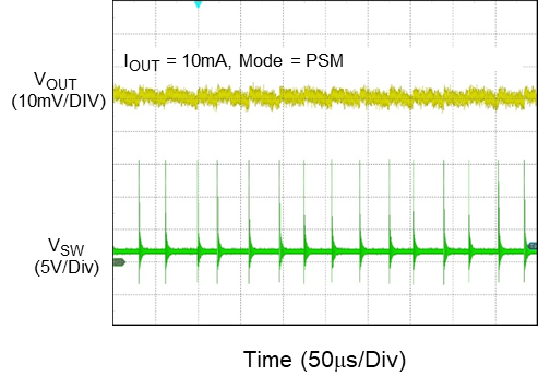
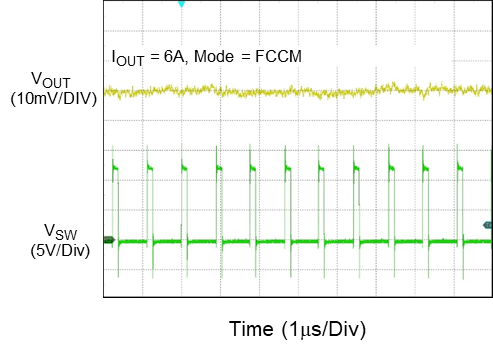
Measure Result
|
Output Ripple Measurement
|
Output Ripple Measurement
|
|
|
|
|
Load Transient Response
|
Load Transient Response
|
|
|
|
|
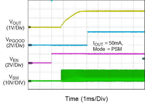
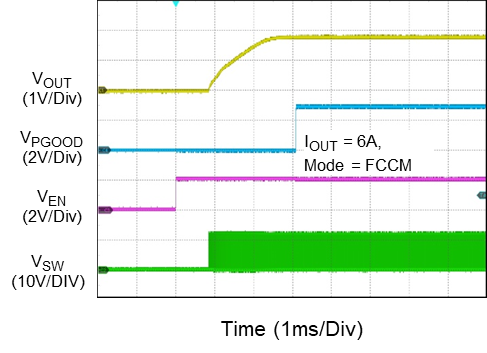
Power On from EN
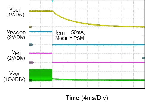
|
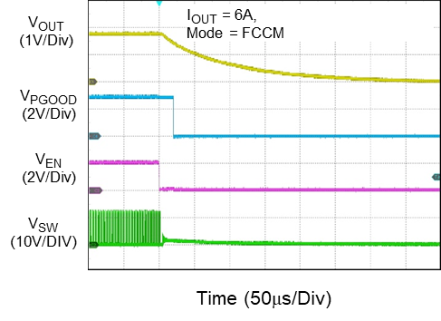
Power Off from EN
|
|
|
|
|
Power On from EN
|
Power Off from EN
|
|
|
|
|
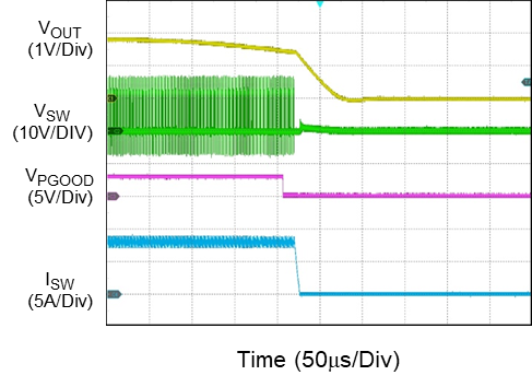
Overcurrent Protection
|
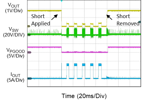
Short-Circuit Protection and Recovery
|
|
|
|
|
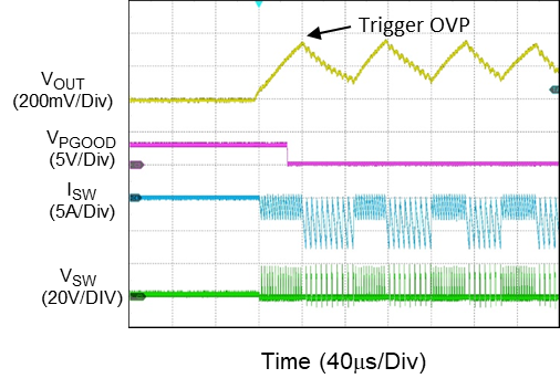
Overvoltage Protection
|
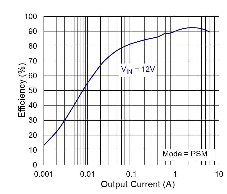
Efficiency vs. Output Current
|
|
|
|
|
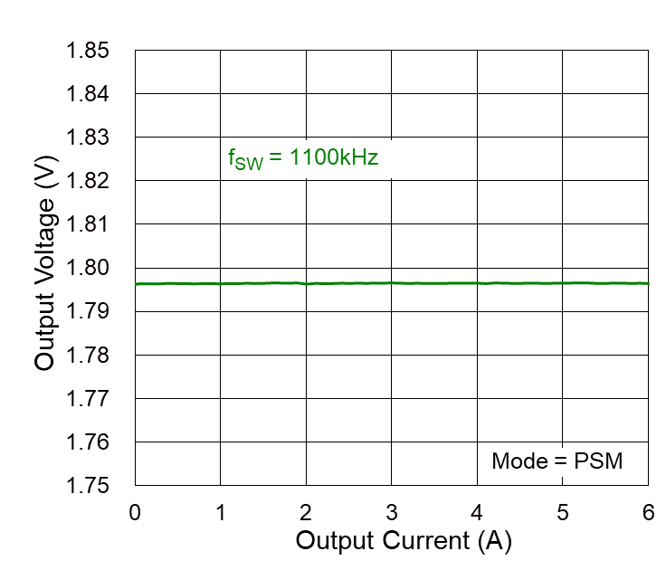
Output Voltage vs. Output Current
|
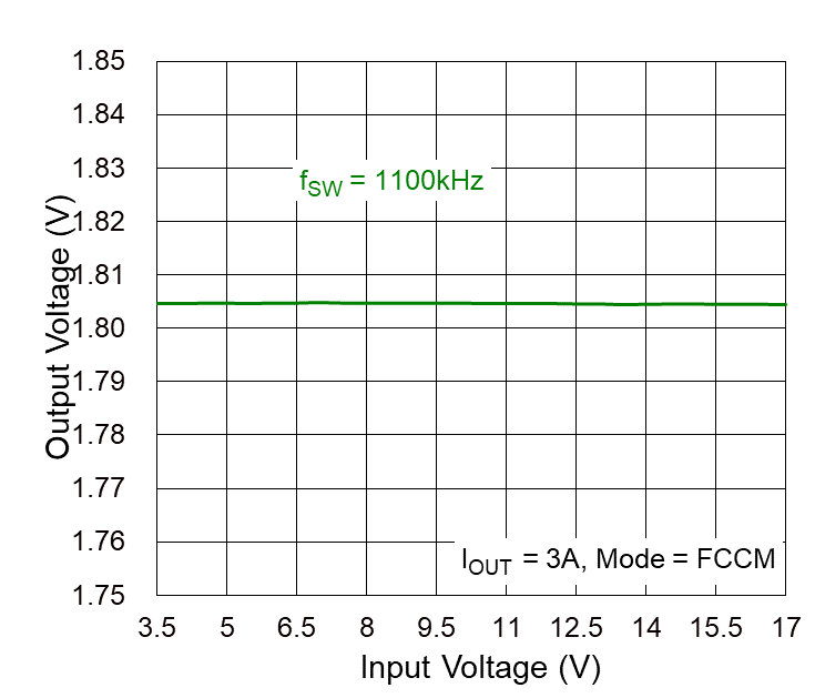
Output Voltage vs. Input Voltage
|
|
|
|
|
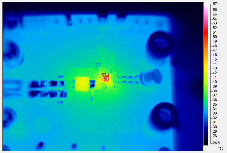
Thermal Image at VIN = 12V, VOUT = 1.8V, IOUT = 6A
|
|
|
Note: Care must be taken to avoid a long ground lead on the oscilloscope probe when measuring the input or output voltage ripple. Measure the output voltage ripple by touching the probe tip directly across the output capacitor.
Evaluation Board Layout
Figures 1 to 4 show the RTQ2806A Evaluation Board layout. This board size is 85mm x 80mm and is constructed on a four-layer PCB, with outer layers of 2 oz. Cu and inner layers with 2 oz. Cu.
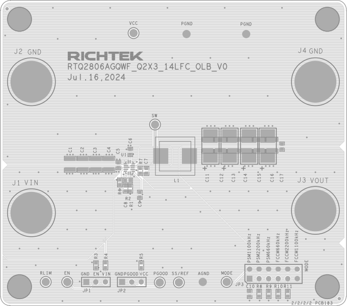
Figure 1. Top View (1st layer)
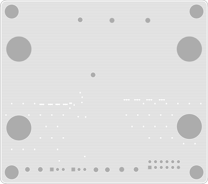
Figure 2. PCB Layout—Inner Side (2nd Layer)
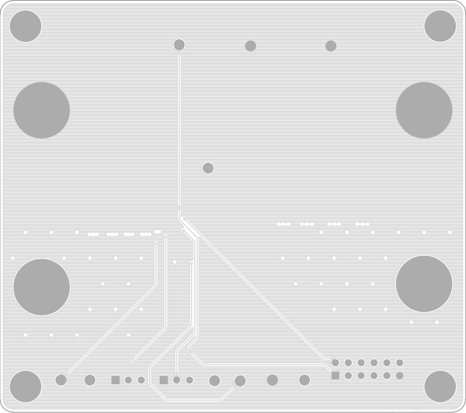
Figure 3. PCB Layout—Inner Side (3rd Layer)
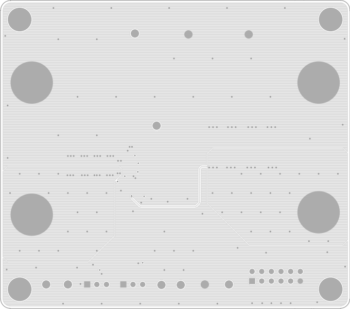
Figure 4. Bottom View (4th Layer)